In the present-day technologically advanced world, chips, or integrated circuits, work as the fundamental building blocks that power the entire devices you rely on daily. From smartphones and laptops to lavish cars and medical equipment, chips are at the centre of modern technology. This post will talk about the intricate world of chip design, exploring the main components and processes involved in creating these small marvels. Come on, once you dig deeper, you find how these chips and even vlsi layout design and more are thoughtfully and tactfully designed to ensure utmost productivity and advancement.
Chip Design basics
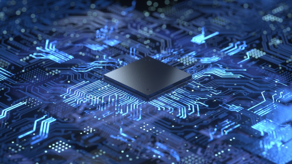
In its spirit, chip design includes transforming complex electrical circuits into compact arrangements of transistors, interconnectedness, and other types of electronic components on a semiconductor material, characteristically silicon. Transistors work as the switches that control the flow of electricity via the circuit, permitting computations and data storage. Chip designers make use of computer-aided design (CAD) tools to develop and simulate these circuits before overall fabrication.
Shrinking Transistors
You may know that Moore’s Law, made by Intel co-founder Gordon Moore, predicts that the number of transistors on a single chip is going to double approximately every two years. This exponential growth has driven the entire miniaturization of transistors, permitting more robust and energy-efficient chips. As transistors shrink, designers experience manifold challenges, including leakage currents, even power consumption, and heat dissipation. Advanced methods like FinFET and even nanowire transistors have come up to overcome these types of hurdles.
Integration or Combined Circuit Fabrication
When the chip design gets complete, it undergoes fabrication in a specialized manufacturing facility, most of the time even called a foundry. This procedure is something that includes multiple steps, including photolithography, deposition, etching, and even doping. Photolithography makes use of light and masks to transfer the circuit design onto a silicon type of wafer, developing multiple layers of transistors and even interconnections. Deposition adds diverse materials, such as metals and even insulators, to form the essential structures, while etching removes an extra level of material to define the circuit components. Doping brings impurities into the silicon to change its electrical properties.
System-on-Chip (SoC) Integration
Since the technology grows and advances, the demand for smaller, more feature-rich devices also increases. System-on-Chip (SoC) integration addresses this type of demand by incorporating multiple functions onto a single chip. SoCs, most of the time, combine processors, memory, graphics, connectivity, and even other kinds of specialized components. Designing such complex chips requires proper consideration of power management, heat dissipation, and even inter-component communication.
Proper Design Verification and Testing
Design verification promises that the chip functions as envisioned before mass production. Simulation, emulation, and even formal verification techniques are used to identify and rectify any sort of design flaws. Additionally, physical testing and characterization confirm the chip’s performance, power consumption, and even dependability. The growing complexity of designs necessitates innovative verification methodologies and even extensive testing processes.
You should also know that design for testability in vlsi is a significant consideration in Very Large Scale Integration (VLSI) chip design. By including DFT techniques, such as scan chains and even built-in self-test (BIST) circuits, professional designers facilitate effective and efficient testing and fault diagnosis during the time of manufacturing, boosting general chip quality and yield.
Memory Design
Memory plays a significant role in chip design, with diverse types such as SRAM (Static Random-Access Memory) and even DRAM (Dynamic Random-Access Memory). Designers experience challenges in balancing memory size, speed, and even power consumption. Advanced memory technologies such as eDRAM (embedded DRAM) and HBM (High Bandwidth Memory) have got developed to address such kinds of challenges and provide higher bandwidth and even capacity for demanding applications.
Power Management and Energy Efficiency
Power management is a significant aspect of chip design, mainly in the realm of portable devices with limited battery life. Designers employ methods such as clock gating, even voltage scaling, and power gating to minimalize power consumption. Energy-efficient architectures, like ARM’s big.LITTLE configuration combine high-performance and even low-power cores to optimize power usage on the basis of workload demands.
Analog and Mixed-Signal Design
Not all types of components of a chip are digital. Many chips include analog and mixed-signal components for functions such as audio processing, signal conditioning, and even sensor interfaces. Designing these types of analog circuits include voltage offsets, addressing noise, and non-linearities. Techniques such as layout optimization, even noise isolation, and calibration get employed to ensure accurate and dependable analog performance alongside digital circuits.
Proper Design for Manufacturability
Chip designers should definitely consider manufacturability across the design process. Design for manufacturability (DFM) techniques have the purpose of optimizing the chip layout and structure to enhance yield and reduce fabrication costs. By considering factors such as process variations, lithography limitations, and metal layer density, designers can boost the chances of successful chip production.
Emerging Trends in Chip Design
Remember that the arena of chip design is constantly evolving, with new trends shaping its overall future. a few of the notable emerging trends can be:
– Neuromorphic Computing: Designing chips that are inspired by the architecture of the human brain, allowing efficient and intelligent procedures for artificial intelligence applications.
– 3D Integration: Stacking diverse layers of chips to boost the overall performance, reduce power consumption, and enable heterogeneous integration of diverse functionalities.
– Quantum Computing: Developing chips that connect the principles of quantum mechanics to carry out computations at a significantly higher speed than classical computers.
– Specialized Accelerators: Designing chips having dedicated hardware accelerators for particular tasks like machine learning, computer vision, and even cryptography to boost performance and energy efficiency.
By highlighting these emerging and growing trends, you can get proper insights into the exciting future possibilities of diverse chip design options.
Conclusion
To sum up, chip design is a remarkable and effective blend of creativity, engineering, and proper innovation. The persistent pursuit of smaller, faster, and even more efficient chips has transformed the world of technology. You can even find the professional hardware design services working on these areas day in and day out to bring better provisions every passing month. As the requirement for advanced electronics goes on to grow, chip designers are certainly going to play a crucial role in shaping the entire future of innovation.